采用锥形波导的偏振转换器
前言
偏振转换器是一类能够将入射光的偏振态从一种形式(例如 TM 模)高效转换为另一种形式(例如 TE 模)的光学器件,在集成光子学和偏振控制应用中具有重要意义。常见的偏振转换器结构包括波导侧壁不对称结构、应力诱导双折射结构、以及采用几何渐变设计的锥形波导等。其中,锥形波导型偏振转换器通过沿传播方向逐渐变化的波导截面,实现不同偏振模之间的平滑能量耦合,从而完成偏振态的高效转换。该结构具有带宽宽、损耗低、对制造误差不敏感等优点,广泛应用于光通信、偏振复用及硅基光子芯片中的偏振控制。

本案例首先利用 FDE 求解器对波导宽度进行扫描,分析 模与 模的有效折射率变化,确定两者发生交叉的区域,以指导锥形波导的设计范围。随后,分别使用 FDTD 求解器和 EME 求解器对整个结构进行三维仿真,通过计算光在锥形波导中的传播过程及偏振转换效率,对比两种求解方法的速度与精度,验证了 EME 在平面波导设计中的独特优势。
仿真设置
模型构建
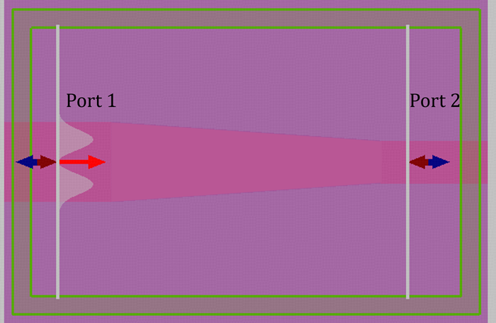
本案例采用 SOI 锥形脊形波导结构,如上图所示。波导基底为玻璃,上覆 厚的的硅层,硅层上方形成 高的脊条。脊条宽度沿着传播方向逐渐变小, 与 的取值将由 FDE 仿真确定。材料折射率取 和 ,与文献[1]保持一致。
光源设置
在 FDTD 仿真部分,使用 Port 端口组作为输入源,模型中包含两个端口,分别位于下图所示的 Port 1 和 Port 2 处,其中 Port 1 为输入端。
由于本案例主要分析 模向 模的偏振转换,因此需要在端口中将 Mode Selection 修改为 User Select 模式。 Port 1 端口选择 模作为入射源, Port 2 端口中同时选择 和 三个模式以记录输出分量。
仿真结果
模式交叉点
打开附件中的 taper_width_sweep.mpps 工程并运行仿真,将前五个本征模式保存至 Modes workspace,以便在后续进行波导宽度扫描时实现模式匹配。随后运行 taper_width_sweep.msf 脚本,脚本将自动对脊条宽度从 扫描至 ,并保存脊条宽度为 时前五个模式的有效折射率( )随宽度的变化。为了消除平板波导部分对 的贡献,使结果中显示的有效折射率变化仅反应脊条结构对模式特性的影响,所得 值需减去平板波导(不含脊条)模式的基准值 。

扫描结果如上图所示, 模与 模的有效折射率曲线在波导宽度约 处发生交叉,该区域为模式耦合与偏振转换的关键宽度范围。
基于 FDTD 计算模式转换率
根据 FDE 仿真结果,在后续的 FDTD 仿真中设置波导输入端宽度 ,输出端宽度 。 这一宽度范围与参考文献[1:1]中的设计保持一致,可确保在锥形波导中有效覆盖 与 模的交叉区域。
Port 1 端口(波导宽度 )选择 模作为输入源, Port 2 端口(波导宽度 )中同时选择 和 三个模式作为输出检测项。附件中的 pol_converter.mpps 工程中包含一个参数扫描,对锥形波导的长度( )进行扫描。
扫描结束后得到 Port 2 端口中的 参数,其中三个模式对应的 参数( 、 、 )分别对应 到 、 到 、 到 的转换效率。
由于仿真计算量较大,附件工程中的扫描范围设定为 。为了更完整地展示模式转换的变化趋势,本文中给出的结果图将扫描范围扩展至 ,如下图所示。
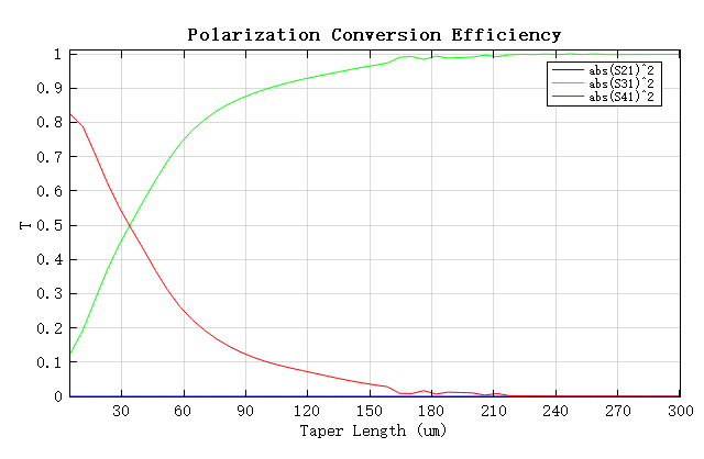
从结果可以看出, 模式几乎未向 模式传递能量;随着锥形波导的长度增加, 模式逐渐转换为 模。当锥形波导足够长时, 模可近乎无损耗地转换为 模,实现高效偏振转换。
基于 EME 计算模式转换率
上文在利用 FDTD 计算模式转换效率时用到了 sweep 功能,为了减少仿真计算量,将附件工程中的扫描范围设定为了 ,扫描点数为51,相当于需要进行51次FDTD仿真,耗时太长,影响仿真效率。因此可以利用本征模扩展(Eigenmode Expansion,EME)求解器进行计算,该方法专为平面波导结构设计,尤其擅长处理大规模、长距离的光传播仿真。
打开附件中的 pol_converter_EME.mpps 工程,运行 Pol_converter_EME.msf 脚本,脚本运行结束后会直接绘制出锥形波导长度为 的模式转换效率,整个过程耗时不到90s。与 FDTD 求解器相比,EME 求解器不仅速度更胜一筹,而且精度也很高。
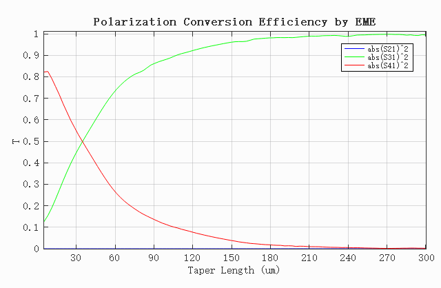
在处理大规模、长距离的光传播仿真时,FDTD 求解器受限于 Courant 稳定性条件,其仿真时间会随结构尺寸的增加迅速增长;相较之下,EME 求解器基于模式耦合理论,将任意输入光场高效分解为波导横截面的本征模式线性组合,并结合边界条件在频域中求解麦克斯韦方程,精确计算模式间的耦合与演化,在保证高精度的同时显著提升计算效率,该方法专为平面波导结构设计,已成为集成光学器件研发中模拟复杂波导系统传输特性的首选工具。