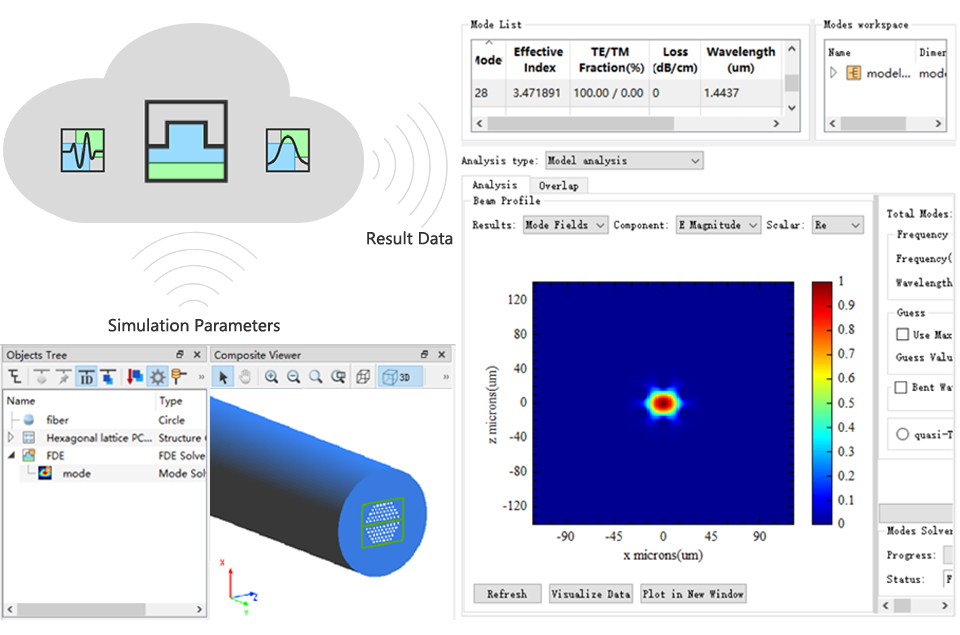
本征模有限差分求解器(FDE)
SimWorks FDE 是研究人员和工程技术人员解决大型集成平面光波导、长距离传输器件和各类新型光纤问题的有力工具。下面,我们会简要介绍FDE求解器的基本原理和主要特色。
FDE算法基本原理
本征模有限差分求解器(FDE)通过在波导类结构截面网格上求解麦克斯韦方程组来计算模式的空间模场分布和频率特性。FDE的基本原理如下:
通过调整频域麦克斯韦旋度方程系数,可将其简化为如下形式:
根据波导中模的基本形式,电磁场可以写作,,代入麦克斯韦旋度方程后得到电磁场分量表达式。如z轴向磁场分量:
在空间内沿坐标轴线性展开,可将上述方程转换为矩阵形式:
电磁场分量的六个矩阵方程可被转换为求解本征值的问题:
矩阵为差分算法的系数矩阵,向量为需要求解的电磁场分量,为传播常数。
在波导结构截面上生成2DYee cell网格后,材料参数、电场和磁场信息均能被体现在每个网格点。本算法使用稀疏矩阵技术进行矩阵本征值求解,可以得到对应于波导结构的模式分布和有效折射率。
-
模式数据
FDE求解器类型为2D Y normal时的仿真结果,如下所示。
- Y轴向量场的空间分布
-
等效折射率
模式的等效折射率(Effective Index)计算如下:
其中是角频率,是模式的传播常数, 是真空中的光速,是模式的群速度,是自由空间的波矢量。
-
TE/TM占比
TE/TM占比(TE/TM fraction (%))表示模式中TE和TM模式能量分布相对大小。其计算公式为:
其中为沿传播方向的电场分量,为沿传播方向的磁场分量,为光波导模式截面上的积分面积。
-
模式损耗
模式的传输损耗(Loss (dB/cm))被计算为:
其中是复折射率的虚部。

模式耦合算法基本原理
模式耦合被用来计算一个波导中某一输入模式与另一个波导中所有模式之间的场重叠和耦合效率。本软件提供的模式耦合算法基本原理如下。
对于某界面输入场、和输出场、,输入和输出功率分别为:
由于波导中任何场都可以看作是由一系列正交模组成的基组成,所以在反射场可以忽略不记的情况下,输入场和输出场可表示为:
其中系数 、由下式进行计算:
由此可以计算出传输输出场的总功率:
第i个模的模式耦合系数()被计算为:
根据模式耦合的结果得知给定的输入场中,第i个模式的场可以携带多少能量。需要注意的是,本算法是基于理想情况进行计算的,对于传输过程中存在反射或者存在损耗的波导时,计算结果可能并不准确。详细介绍请见Snyder和Love的《光波导理论》。
求解器的主要特色
3D CAD界面和丰富的零件库
- 多多视角3D Computer-aided Design(CAD)工作平台,助力模型搭建。
- 内置丰富的波导结构库,能够快速搭建各种结构的波导。
- 支持Graphic Design System(GDS)版图文件的直接导入,方便调整复杂结构。

网格技术
- 支持自动非均匀网格、自定义网格等网格剖分技术,提高复杂波导结构截面2D Yee cell网格构建效率。
- 拥有当前流行的高精度共形网格细化技术,包括:体平均偏振相关的等效介电常数法(Volume-average polarized effective permittivity)、体平均法(Volume average)、Yu-Mittra 1、Yu-Mittra 2,以达到更精确的模式求解结果。
边界条件
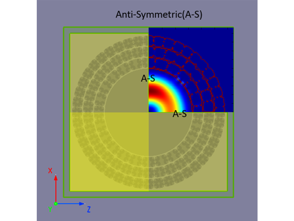
- 提供多种仿真边界条件,如完美匹配层(PML)、周期、对称/反对称、完美电导体(PEC)/完美磁导体(PMC)。
频率分析
- 结构所有的模式均可进行数据可视化,并进行频率分析。
- 模式耦合功能方便用户分析模式重叠及计算模式之间的耦合效率。
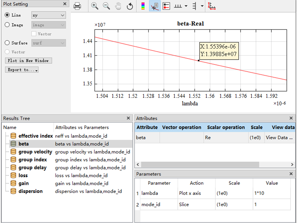
- 支持频率扫描分析,快速获取模式群速度、损耗、色散等关键数据。
脚本控制
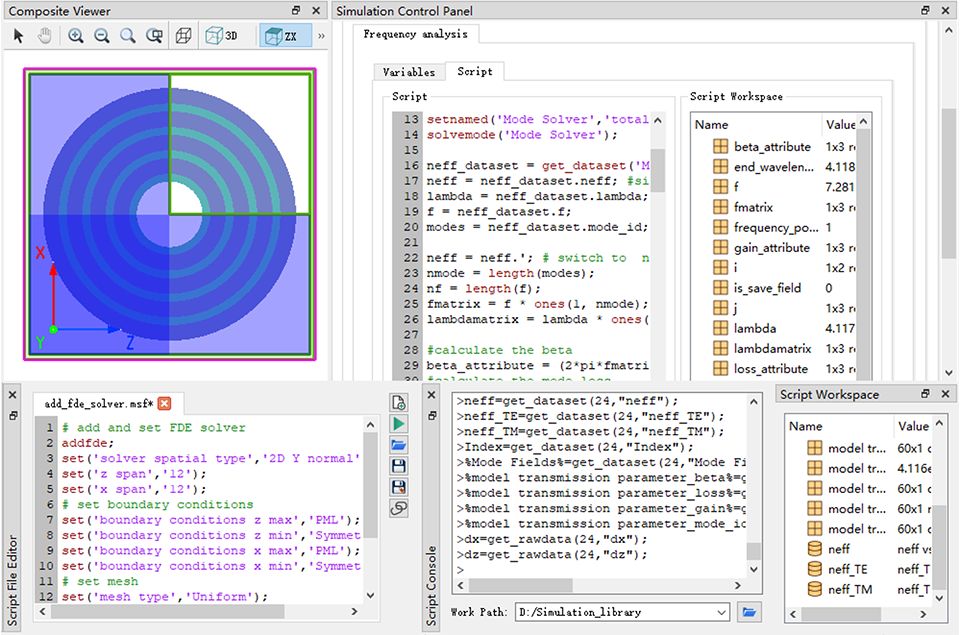
- 脚本功能允许用户操纵仿真中的每一个步骤,实现参数化的构建,为用户提供新的交互体验。
- 软件内置完整的函数库,允许自定义函数,基本满足数学计算的所有需求。
强大的算力
- 在OpenMP、MPI、AVX等多种并行计算技术的加持下,算力及模式求解速度都得到了高效提升。
- 为用户提供云端模式求解服务,不再局限于本地计算资源。
领先行业的超高计算精度
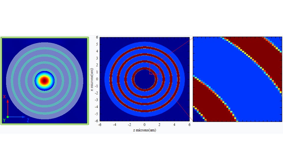
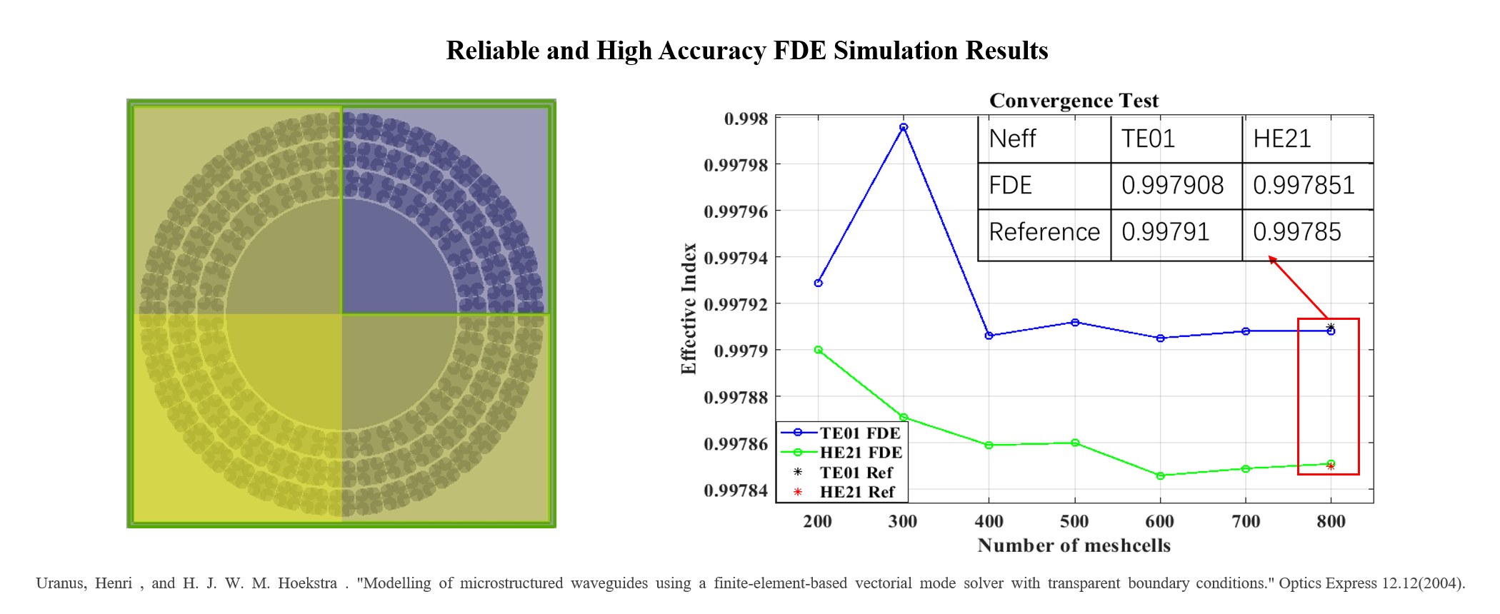
- 本征模有限差分算法利用模式耦合对光波导进行模式求解,能够得到高精度的模式求解结果。以空心光子晶体光纤的模式求解为例,如下图所示,可以看到该结构对网格的微小变化十分敏感。经过收敛性测试后,有效折射率结果与文献的相对误差稳定在0.0001%,展示了SimWorks FDE算法的超高计算精度。
参考文献
[1]Zhaoming Zhu and Thomas G. Brown, "Full-vectorial finite-difference analysis of microstructured optical fibers," Opt. Express 10, 853-864 (2002)