有机发光二极管
前言
有机发光二极管(OLED)器件因其自发光特性、宽视角、高对比度以及可实现柔性显示等优势,已广泛应用于高端显示和固态照明领域。典型的 OLED 结构由多层有机功能薄膜与电极构成,器件整体厚度通常处于亚微米量级。在这种多层介质环境中,发光层内偶极子源产生的辐射会受到显著的光学约束和干涉效应影响;同时,由于各功能层之间存在因折射率不连续,光在传播过程中容易以波导模或表面等离激元模的形式被限制在器件内部,只有少部分光能够有效辐射到空气中。因此,如何通过精确建模多层薄膜的光学行为,并结合微纳结构设计提升光提取效率,是 OLED 光学设计中的关键问题。
本案例使用 2D FDTD 对 OLED 器件进行建模,通过对比无微结构与引入周期性微结构(光子晶体)的两种情形,评估微结构设计对光提取效率的提升效果。
仿真设置
模型简介
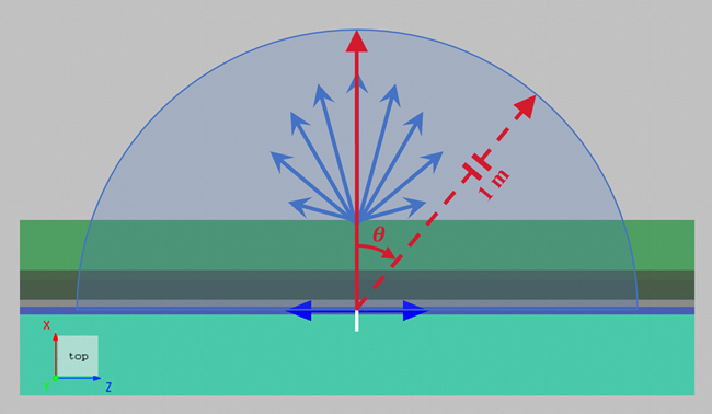
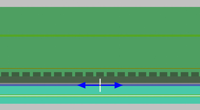
本案例采用的仿真模型基于典型的平面 OLED 多层薄膜结构,自下而上依次包括铝(Al)阴极、三(8-羟基喹啉)铝(Alq₃)有机层、a-NDP 有机层、氧化铟锡(ITO)透明阳极、氮化硅(SiN)缓冲层以及玻璃基底。其中,在 SiN 层与玻璃基底之间引入周期性调制的氮化硅光子晶体(Photonic Crystal, PC)结构,用以调控器件的出光行为并增强光提取效率。
发光层位于 Alq₃ 有机层中,并被建模为波长范围为 的电偶极子光源,用以表征 OLED 中自发辐射发射体的光学行为。
为了模拟实际 OLED 器件中大量发射体非相干、近似各向同性取向的辐射特性,仿真中采用多次电偶极子源激发的方式进行统计平均处理。具体而言,通过在发光层内改变电偶极子源的空间位置与取向方向,分别计算不同偶极子构型下的辐射场分布;随后对各取向条件对应的仿真结果进行加权求和,从而获得等效于实际器件整体发射行为的平均辐射响应。
仿真结果
辐射特性与光提取效率
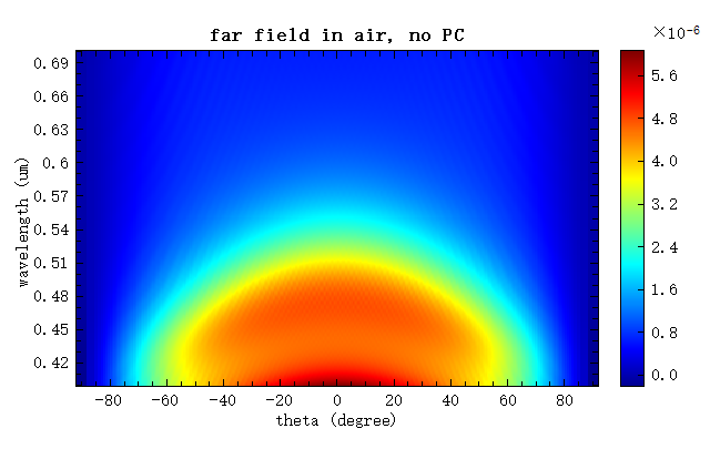
附件中的 OLED_no_pattern.msf 脚本可自动调整电偶极子的方向并运行仿真,得到不含光子晶体结构时的仿真结果。工程中的 Far field change index 分析组基于远场投影方法计算了在空气中的远场角分布,如下图所示。该分析组在计算过程中考虑了远场传播过程中玻璃与空气的界面处发生的反射与折射现象。
对应的辐射功率分数如图所示。其中 “Total emitted power” 表示发光层中偶极源产生的总辐射功率,“Emission reaching glass” 表示能够从 OLED 有机层传播至玻璃基底中的辐射功率,而 “Emission into air” 则对应最终成功耦合并辐射到空气中的功率分数。
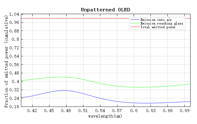
可以看出,仅有少部分辐射功率能够最终耦合至空气中。尤其是在波长约 附近,进入空气的功率分数小于 ,表明该波段的辐射主要受限于器件内部的光学模式,光提取过程受到较强限制。
光子晶体对 OLED 辐射特性的影响
附件中的 OLED_pattern.msf 脚本可自动激活工程中的光子晶体结构,并调整电偶极子的位置以及方向,得到包含光子晶体时的仿真结果。空气中的远场角分布如下图所示,可以观察到引入光子晶体后,器件的辐射模式以及其随波长变化的特性均发生了明显改变。
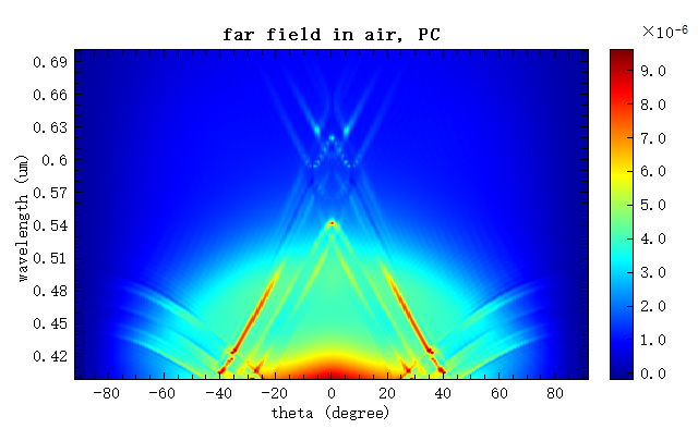
对应的辐射功率分数如图所示,与无光子晶体结构相比,引入周期性氮化硅光子晶体后,空气侧的辐射功率分布发生了明显变化。可以观察到,在波长约 附近,进入空气的辐射功率分数显著增加。这一结果表明,光子晶体结构通过调控器件内部的光学模态分布,使部分原本受限于多层结构中的辐射更有效地耦合至自由空间,从而改善了对应波段的出光性能。
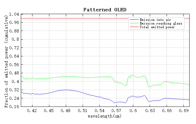
由此可见,引入光子晶体结构能够在特定波长范围内有效增强 OLED 向空气中的出光能力,为光提取效率的进一步优化提供了可行的设计思路。
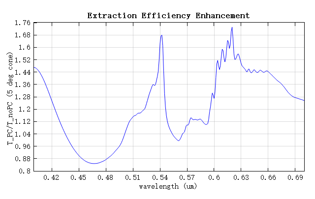
光提取率的提升
光提取效率的提升通过比较有光子晶体与无光子晶体两种情形下的提取效率进行评估,其定义为:
附件中的 OLED_enhancement.msf 脚本根据两种结构在空气中的远场分布,计算了逃逸至空气中的光在5度锥形区域内的提取效率提升情况,如下图所示。结果表明,引入光子晶体结构后,可以在特定波长范围内显著提高 OLED 的光提取效率。