石墨烯材料
石墨烯材料 #
本节是关于石墨烯材料的介绍。
石墨烯材料 #
石墨烯是一种超薄(单层原子厚度)的光学材料。通常,使用表面电导率σ而不是介电常数ε来表征。基于 Hanson G W 的文章,在忽略磁场存在的情况下,石墨烯材料的表面电导σ(f,μc,Γ,T)为:
σ(f,μc,Γ,T)=σintra(f,μc,Γ,T)+σinter(f,μc,Γ,T)
σ(f,μc,Γ,T)的第一项即为带内电导率σintra(f,μc,Γ,T):
σintra(f,μc,Γ,T)=πℏ2(2πf−j2Γ)je2∫0∞ξ(∂ξ∂fd(ξ)−∂ξ∂fd(−ξ))dξ
第二项为带间电导率σinter(f,μc,Γ,T):
σinter(f,μc,Γ,T)=πℏ2je2(2πf−j2Γ)∫0∞((2πf−j2Γ)2−4(ξ/ℏ2)fd(ξ)−fd(−ξ))dξ
其中,fd(ξ)为费米-狄拉克分布,fd(ξ)=1/[1+e(ξ−μc)/kBT]。
这里:
| Symbol | Name | Units |
|---|---|---|
| f | 频率 | Hz |
| ξ | 能态(ξ=ℏω/2) | J |
| Γ | 散射率 | eV |
| μc | 化学势 | eV |
| T | 温度 | K |
| e | 电子电荷 | C |
| ℏ | 约化普朗克常数 | ℏ=6.62607015e−34J⋅s |
其中,以下四个参数的数据支持用户输入:
| Name | Symbol | Units | Range | Default | Description |
|---|---|---|---|---|---|
| Scattering rate | Γ | ~ | 实数,Γ≥1 | 0.00051423 | 散射率Γ,Γ=1/(2τ)。 |
| Chemical potential | μc | eV | 实数,μc≥0 | 0.64 | 化学势。 |
| Temperature | T | K | 实数,T≥0 | 300 | 温度。 |
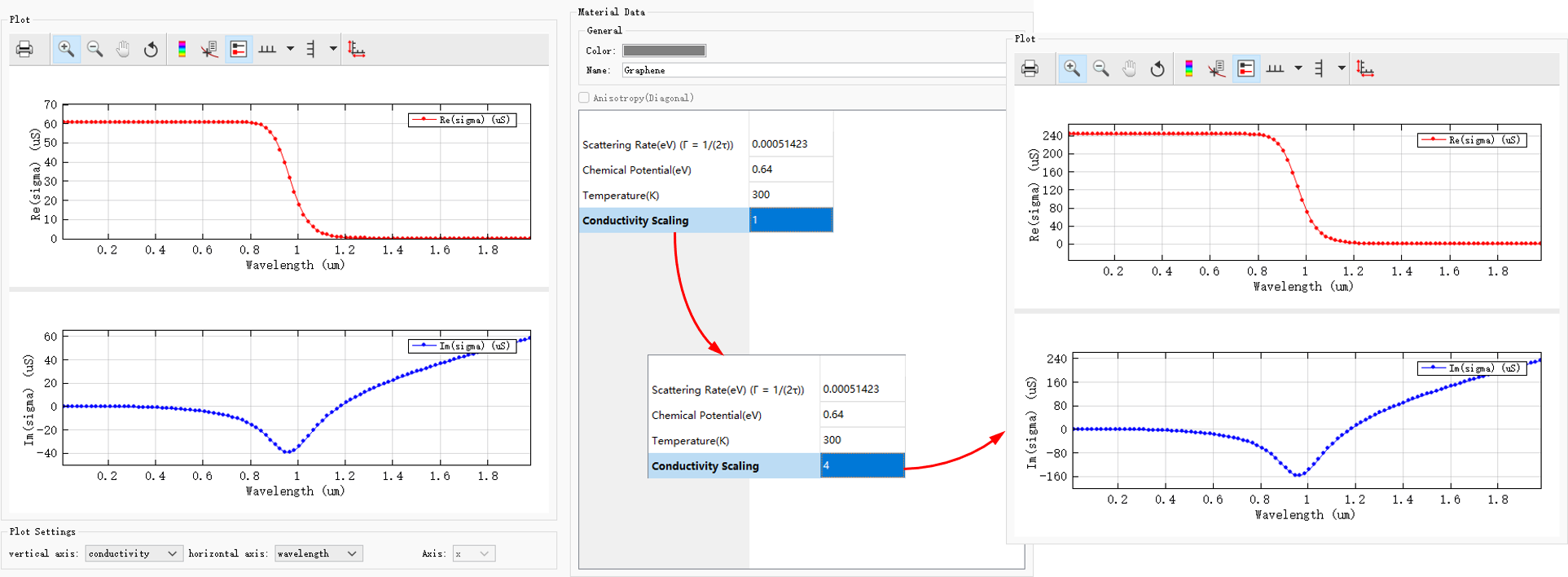
| Conductivity scaling | c | ~ | 实数,c≥0 | 1 | 电导率比例系数。 |
上述提及的石墨烯表面电导公式适用于单层石墨烯材料。对于多层石墨烯材料,可以通过调节电导率比例系数改变总电导率来实现。
材料设置 #
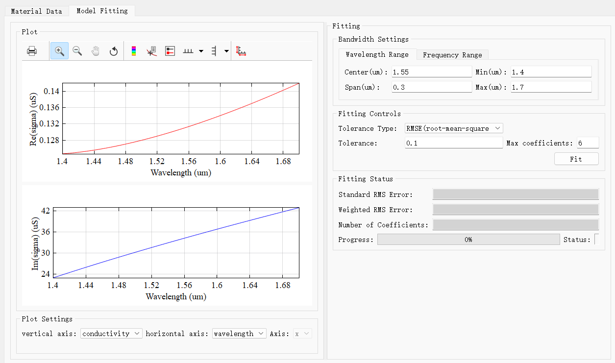
在材料库窗口,通过Add material>Add new material>Add graphene添加石墨烯材料模型,在弹出的编辑界面修改石墨烯模型的材料参数(请见上图)。切换到材料拟合页面,可以观察材料拟合模型在对应波段是否拟合正确。
更多信息 #
- 石墨烯材料模型仅允许赋予 2D 结构。
- 石墨烯材料不支持各向异性。
- 石墨烯材料是一种特殊的 2D 材料,与一般的材料不同,无需在石墨烯处添加高精度的网格,即可实现石墨烯的精确仿真。
因其独特的光学、电学和机械特性,石墨烯已成为多个研究领域的热点材料。一个典型的案例见在石墨烯中激发表面等离子体。
案例:基于石墨烯的可调谐太赫兹超材料 #
石墨烯是厚度为一个原子的单层碳材料,由于其独特的物理特性,可以被应用于纳米级等离子体系统。通过调整静电掺杂或费米能级来激发单层石墨烯的等离子波,从而实现对光的操纵和控制。详情请参阅石墨烯超材料。
参考文献 #
[1] Hanson G W. Dyadic Green’s functions and guided surface waves for a surface conductivity model of graphene[J]. Journal of Applied Physics, 2008, 103(6): 064302.
[2] Falkovsky L A. Optical properties of graphene[J]. Journal of Physics Conference Series. 2008, 129: 012004.