2.5D 求解器
2.5D 求解器 #
本节是关于2.5D基本原理以及时域有限差分(FDTD)和频域有限差分(FDFD)求解器独有的2.5D求解器设置的介绍。
2.5D时域有限差分求解器(FDTD) #
2.5D时域有限差分求解器被集成在FDTD solution当中,当用户在FDTD的Dimension and Polarization选项中选择2.5D时,该求解器将自动启用,并显示出2.5D settings选项卡,供用户进行相关的配置。该求解器适合用于模拟较大尺度(数百微米)下的三维器件,特别是那些在高度方向上结构和材料完全不变或者仅有几个离散变化的结构。较大尺寸的器件对于3D FDTD求解器来说会占用大量的内存和计算资源,相比之下,2.5D时域有限差分求解器在处理这类器件时能够显著节省内存和计算资源。目前该求解器在平面波导领域计算效果非常好,通过对第三维度的折叠和网格细化来运行2D FDTD,这将极大的节约用户器件设计以及仿真计算的时间。
计算原理与方法 #
2.5D时域差分求解器的基本原理是,将三维几何体材料通过等效折射率方法生成新的二维材料来代替原本的结构,从而将3D问题简化为2D问题。该理论方法基于Hammer和Ivanova提出的一种有效折射率变分法[1],通过在侧向的高度上进行解模求解等效的2D材料系数,进而进行2D FDTD仿真。同时,在进行宽带仿真时,由于不同频率下的有效折射率不同,新材料将具有色散特性,这种特性一部分来自于原始材料的性质,另一部分则来自于形状的压缩。其具体方法如下所示:
εeffTE(x,y,ω)=(kβr)2+∫yχr2dy∫y(ε(x,y,z)−εr(y,ω)χr2)dy
εeffTM(x,y,ω)=(kβr)2⋅∫yε(x,y,z)1χr2dy∫yεr(y,ω)1χr2dy+k2∫yε(x,y,z)1χr2dy∫y(εr(y,ω)1−ε(x,y,z)1)(∂yχr)2dy
其中βr,εr,χr来自于侧向高度上一维的传播常数,相对介电常数以及模式分布。该变分法最主要的假设是忽略了平板波导模式在垂直方向上的耦合,此时波导将仅支持互相垂直的TE、TM模式,从而将其近似为二维仿真。
2.5D时域有限差分求解器的流程如下所示:
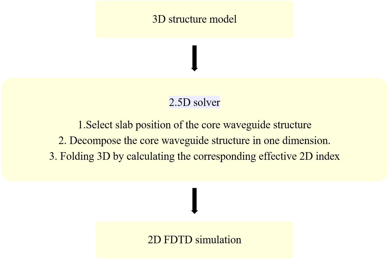
以下将对2.5D求解器当中几个步骤进行详细说明。
- 对于步骤1,用户需要在2.5D settings标签页当中进行设置,相关设置参阅本页面下平板波导的位置部分。用户应当慎重选择该位置,这将直接影响后续解模有效折射率的正确与否,所选择的位置在高度上需要尽量覆盖用户研究的所有结构;
- 对于步骤2,用户可以选择将等效材料设置为窄带介质材料或宽带色散材料,同时还需要设置合适的解模数量(Total Modes),更多相关设置,请参阅本页面下的波导色散 以及平板模式部分。解模结果将展示在Wave shape页面,用户需要仔细选择所要研究的模式,因为这将影响最终计算得到的等效材料结果;当用户仅需要获得单频点或窄带的等效材料时,可选择Narrow Bandwidth(Ignore Waveguide Dispersion) 选项,但若仿真的工程对色散敏感或者仿真的材料色散较大时,则需要勾选Broad Bandwidth进行计算等效的2D色散材料;之后,用户还需要输入Number of samples (wavelength points) 的值,该项用于材料拟合,输入的点数越多,等效的2D色散材料将拟合得越精确;
- 步骤3中建立2D有效折射率的过程将由软件自动进行,软件会建立2.5D材料专有的材料库,用户可以点击Material选择Open check material library打开专有材料库,查看Slab position以及Test position处的有效折射率。此时Index monitor的结果中也将显示等效后的有效折射率。
除上述说明以外,用户还需要注意,当使用2.5D求解器时,3D结构将被折叠为2D平面,此时的FDTD求解器以及监视器当中的高度选项(软件当中默认情况下为y方向)将没有意义,监视器放置在任意高度下结果都将一致。
案例说明 #
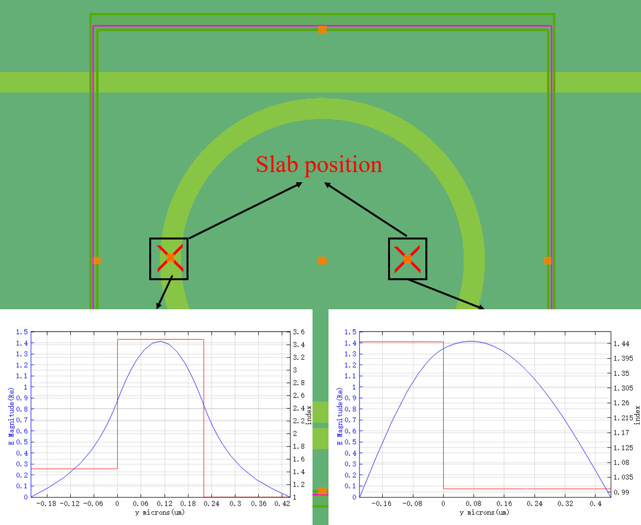
以案例硅基双直波导微环谐振腔作2.5D仿真说明,该谐振腔由硅材料组成,基底为二氧化硅。
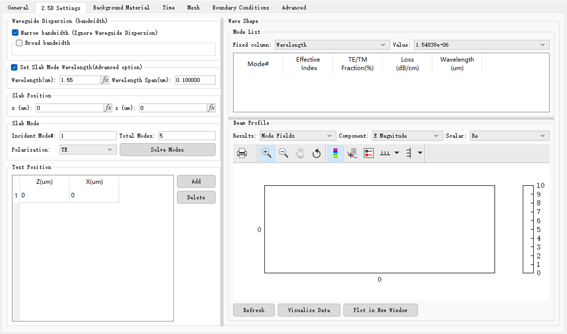
在选择2.5D后,将出现以下新的2.5D settings页面,该页面可以选择平板波导解模位置以及宽带等设置。
由于入射光主要在硅圆环谐振腔当中进行传播,slab position应当选择谐振腔所在位置进行计算。下图展示了不同位置的基模结果。
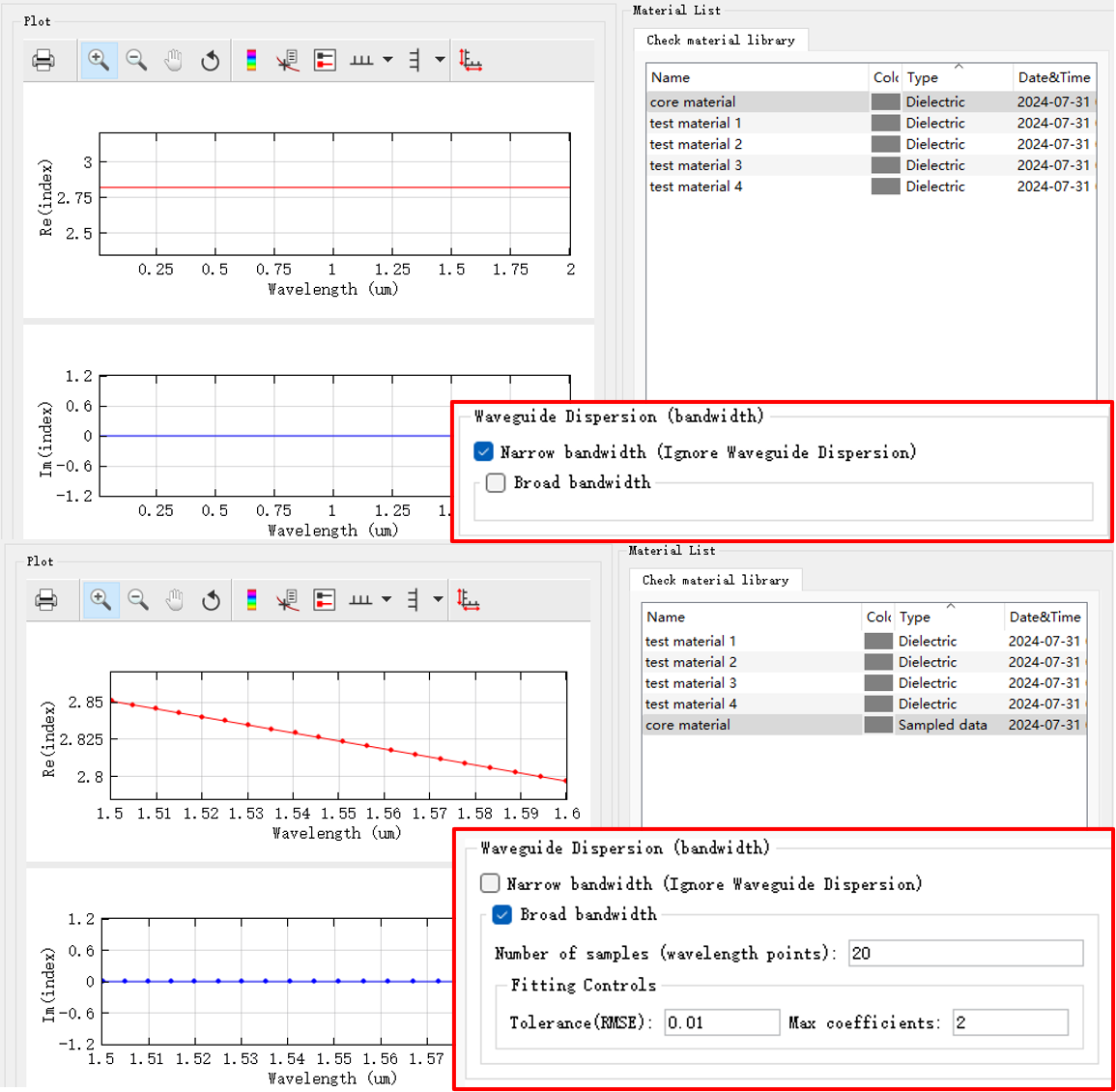
在本案例当中需要得到多频点下的传输效率,因此需要选择宽带进行仿真,同时选择基模进行仿真,用户可以在Open check material library中看到core点以及test点等效折射率在宽带窄带中计算的变化。
2.5D频域有限差分求解器(FDFD) #
2.5D频域有限差分求解器(FDFD)依然集成在FDFD solution当中,压缩维度的原理方法与2.5D时域有限差分求解器一致,设置完2.5D专有页面后,其它设置页面都是通用的,不再赘述,直接运行仿真即可。
2.5D求解器设置 #
波导色散 #
*Waveguide dispersion (bandwidth)*选项卡用于设置等效2D材料的带宽。
| Name | Description |
|---|---|
| Narrow bandwidth (ignore waveguide dispersion) | 窄带仿真;该选项适用于单频仿真或仿真带宽很窄的情况。材料特性仅取仿真带宽的中心频率。 |
| Broad bandwidth | 宽带仿真;勾选该选项启用宽带仿真,需设置材料拟合的参数。 |
| Number of samples (wavelength points) | 当Broad bandwidth勾选时启用该项,用于设置材料拟合的波长点数量。 |
| Tolerance(RMSE) | 当Broad bandwidth勾选时启用该项,用于设置拟合模型和材料样本点之间允许的最大公差。 |
| Max coefficients | 当Broad bandwidth勾选时启用该项,用于设置拟合模型多项式允许的最高阶数。 |
设置平板波导的波长(高级设置) #
Set slab mode wavelength (advance option) 选项卡用于指定平板波导解模的波长,勾选以启用该项。
平板波导的位置 #
Slab position选项卡用于设置平板波导解模中心的位置坐标 (x, z) 。
平板模式 #
| Name | Description |
|---|---|
| Incident mode# | 注入模式的编号;解模完成后,显示模式列表中作为注入模式的模式序号。 |
| Total modes | 模式总数;模式列表中返回模式的最大数目。 |
| Polarization | 偏振态;下拉选择 TE/TM 偏振。 |
| Solve modes | 解模。 |
测试位置 #
Test position选项卡创建材料测试点的 (z, x) 坐标。
| Name | Description |
|---|---|
| Add | 添加测试点坐标。 |
| Delete | 删除测试点坐标。 |
波形 #
Wave shape选项卡包括模式列表和分量。
- 模式列表
Mode list显示解模得到的模式信息。
| Name | Description |
|---|---|
| Mode# | 模式序号。 |
| Effective index | 模式的等效折射率。 |
| TE/TM fraction(%) | 模式中 TE 和 TM 模式能量分布相对大小。 |
| Loss | 模式的传输损耗;即光信号在波导器件中由于吸收、散射等因素引起的能量衰减。 |
| Wavelength | 模式对应的波长。 |
- 分量
Component用于选择绘图窗口的场分量以及对所选场分量的进行运算。
| Name | Description |
|---|---|
| Component | 选择绘图窗口的场分量; TE: Ex, Hy, Hz; TM: Ey, Ez, Hx。 |
| Scalar | Abs:所选场分量的模; Re:所选场分量的实数部分; Im:所选场分量的虚数部分; Phase:所选场分量的辐角。 |
参考文献 #
Hammer M , Ivanova O V .Effective index approximations of photonic crystal slabs: a 2-to-1-D assessment[J].Optical and Quantum Electronics, 2009, 41(4):267-283. ↩︎