威尔金森功分器
前言
威尔金森功率分配器是一种可用于功率分配的三端口器件,相比于普通T型功率分配器,它可以使所有端口的阻抗相匹配,并且可以按任意比例分配功率。与电阻功率分配器相比,威尔金森功分器可以实现输出端口之间的隔离,且没有损耗,只有输入信号在输出端口产生的反射波会被电阻元件耗散。本案例建模仿真了 Pozar[1] 中例7.2设计的均等分配(3 dB)威尔金森功分器。
仿真设置
模型设置
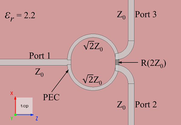
本案例中使用的威尔金森功分器结构如上图,其中 为输入端口, 及 为输出端口。整个结构由放置在衬底上的金属传输线以及电阻器组成,其中衬底的厚度为 ,相对介电常数为 。Pozar[1:1] 中微带传输线的尺寸与特性阻抗的公式3.196如下:
其中 为传输线的宽度, 为衬底厚度, 为微带传输线的有效介电常数。微带传输线的有效介电常数近似为:
其中 为衬底的相对介电常数。根据以上公式以及每段传输线的特性阻抗值可以计算出每段传输线的宽度 ,分别为 和 。
结构中的传输线和电阻器的厚度远小于工作波长,因此可以使用2D结构来建模。阻抗为 的环形传输线可以由二维多边形构成,其周长为 。电阻器使用二维矩形来建模,材料为集总元件
光源设置
本案例中使用Port端口组作为输入源,添加三个端口分别位于下图中 、 和 的位置。该器件的设计频率为 ,因此我们将光源的频率范围设置为 。
端口可以同时充当模式源和FDFP监视器,通过模式拓展功能可以计算出器件的S参数。三端口器件的S参数包含九个元素,如下:
要获得器件的所有S参数项,必须进行多次仿真。由于该器件具有互易性()和对称性,我们只需要两次仿真就可以确定所有的S参数,两次仿真分别由 和 作为源端口。
求解器设置
求解器的 边界使用PEC边界条件,用于模拟器件的接地平面,其余边界条件均为PML。当 作为输入源时,由于光源以及结构的对称性,我们可以在 使用Symmetric对称边界条件将仿真区域缩小至1/2,从而减少仿真时间,如下图所示。

仿真结果
电场分布
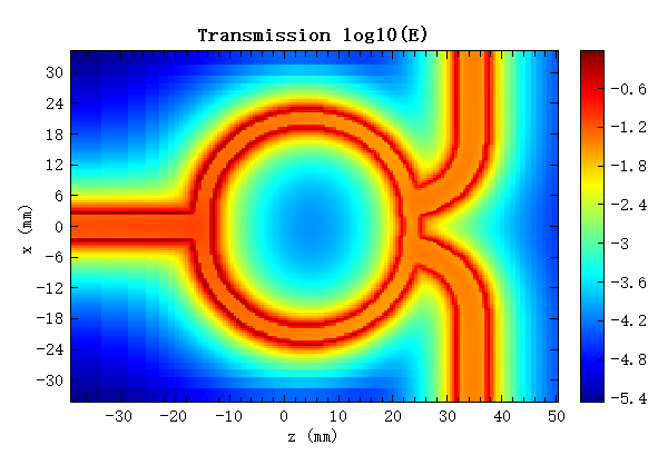
下图展示了传输和隔离仿真中,频率为 时器件的电场分布。当 作为源端口时,由于对称性, 与 处的电场强度一致。当 作为源端口时, 处的电场强度很小,体现出 与 之间明显的隔离性。

S参数
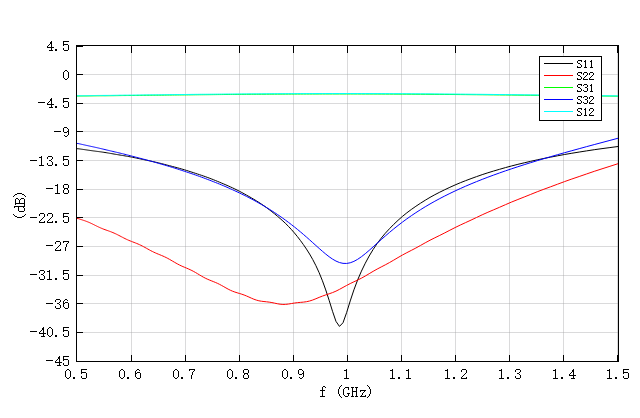
威尔金森功分器的S参数如下图所示,其中心频率为 ,与设计频率 相差小于1%。在频率为 处, 、 ,说明该器件在设计频率下,从任意端口输入得到的反射都非常小,表明端口之间的阻抗匹配良好。 ,说明器件从 输入传输到 端口的功率非常小,体现了输出端口之间具有良好的隔离性能; ,且在整个仿真频段内变化小于10%,说明从输入端口( )传输到 的功率,在全波段均大约为50%。由于器件的对称性,输入端口传输到 的功率也为50%,体现了器件的等功率分配以及良好的带宽。