硅纳米线阵列波导光栅
前言
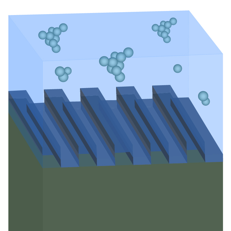
阵列波导光栅是密集波分复用系统中的关键器件,随着大规模光子集成器件的发展,阵列波导光栅的小型化设计成为了重要的课题。硅纳米线具有较高的芯层-包层折射率差,可以将光限制在更小的波导内,在同样的弯曲损耗下可减小波导的弯曲半径,在相同的串扰下可减小阵列波导的间隔,从而减小阵列波导光栅器件的尺寸,有利于器件的集成。
本案使用 2.5D-FDTD 求解器例建模仿真了如下图所示的马鞍型硅纳米线阵列波导光栅,并计算了其输出的频谱响应与损耗。这主要是因为阵列波导光栅尺寸较大,3D-FDTD 仿真会占用大量的计算机资源并耗费大量的仿真时间。而 2.5D-FDTD 则利用垂直方向结构不变等效出相应的新材料,将 3D 问题转化为 2D 问题,从而在保证仿真精度的前提下大大简化了仿真。
仿真设计
结构设置
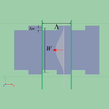
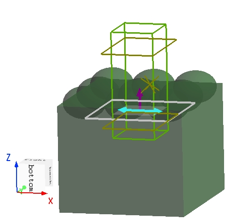
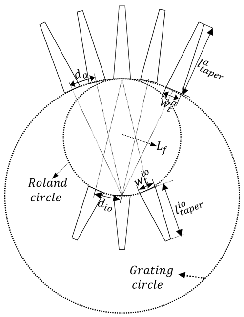
本案例中硅纳米线阵列波导光栅的设计参考了文献[1],使用一个输入波导和三个输出波导。设计中引入三个假设:(1)材料参数取室温下中心波长的 TE 基模的值;(2)罗兰圆的直径远大于输入/输出/阵列波导在输入/输出耦合器处的芯-芯距离;(3)弯曲波导与直波导的有效折射率、群折射率的差异可以忽略。本案例所采用模型结构如下图所示,其工作的中心波长 为 、信道间隔 为 。
| 参数 | 符号 | 值 |
|---|---|---|
| 自由频谱宽度 | ||
| 直波导宽度 | ||
| 阵列波导数 | ||
| 平板波导处各输入/输出/阵列波导的芯-芯距离 | , | |
| 连接阵列波导与平板波导的锥形渐变波导在光栅圆的宽度 | ||
| 连接输入/输出波导与平板波导的锥形渐变波导在罗兰圆的宽度 | ||
| 锥形渐变波导的长度 | ||
| 输入/输出波导的长度 | ||
| 弯曲波导半径 | ||
| 最短阵列波导中的直波导的长度 | ||
| 罗兰圆直径 | ||
| 相邻阵列波导长度差 |
求解器设置
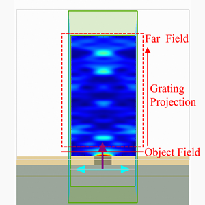
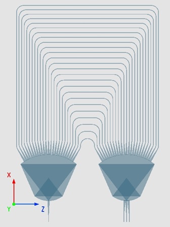
阵列波导光栅的阵列波导部分只包含稳定传输的波导结构,可以认为光在阵列波导中传输时,光场的模式不会发生改变,只有振幅和相位发生变化。因此可以将阵列波导光栅分为输入平板波导区域和输出平板波导区域分开进行仿真,如下图。这样可以大大减少仿真区域,从而进一步减少仿真时间。
光源
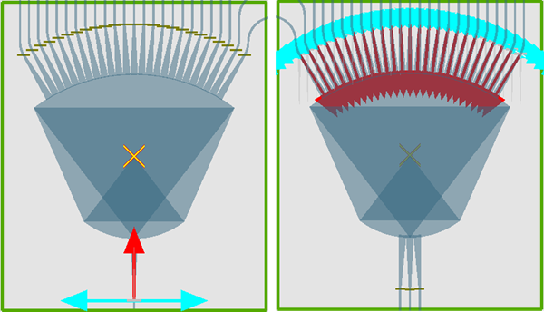
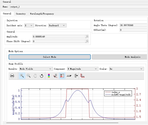
因为我们将阵列波导光栅仿真分为两部分,所以在进行输出波导区域的仿真时,每根阵列波导的光源必须保证和光源经过输入平板波导耦合到每根阵列波导的模一致。从上图中可以看到,光经过阵列波导后到达输出波导的锥形波导时带有一定的角度,因此我们需要设置模式源的注入方向与锥形波导中轴的角度一致。我们的模式源将会自动计算出当前方向上的传播模式。
我们还需要设置模式源的振幅,使其与从输入波导耦合到每一根阵列波导中的光透射率相匹配。而阵列波导长度差引起的相位延迟可以通过调整模式源的脉冲延迟来代替,模式源的脉冲延迟设置公式如下:
其中, 为相邻阵列波导的长度差, 为阵列波导的群折射率, 为真空中的光速。
仿真结果
输入平板波导仿真结果
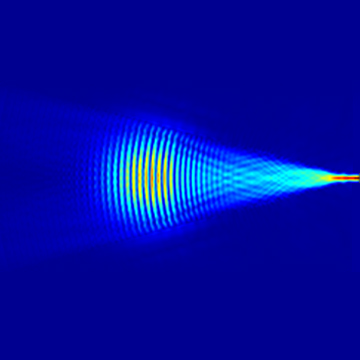
通过放置在硅板中的FDFP监视器,可以得到波长为 的光从输入波导进入器件后传播到阵列波导的电场分布,如下图。从图中可以看出,光从输入波导耦合到输入平板波导区域并扩束,自由传播到罗兰圆的边缘,随后耦合进阵列波导。
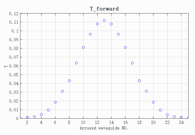
光从输入波导进入器件后,耦合到阵列波导中的透射率可以通过每一根阵列波导中的FDFP监视器得到,下图显示了 波长的光在每一根阵列波导中的透射率。从图中可以看到,输入光的大部分能量都耦合进了阵列波导。
输出平板波导仿真结果
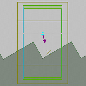
查看最左侧模式源注入的模式,如下图。可以看到,模式源在具有角度的时候依然可以正确地解模。
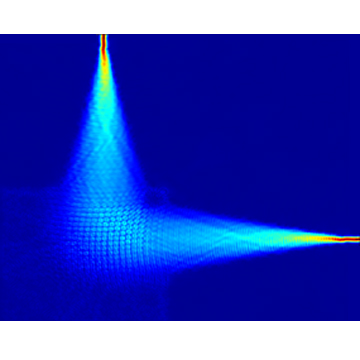
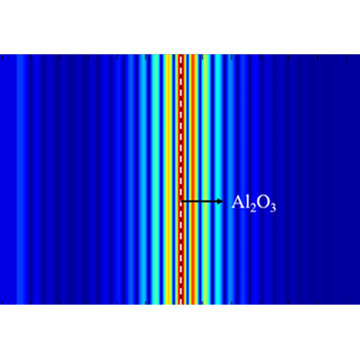
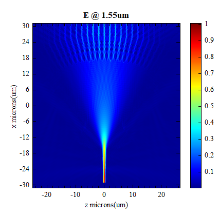
通过放置在硅板中的FDFP监视器,得到的波长为 的光的电场分布如下图,可以看到多个光源的光从阵列波导中输入,耦合进罗兰圆后发生衍射,最终在输出波导的边缘汇聚成一束较强的光,耦合进输出波导。在最强的衍射光两侧还存在着两束较弱的衍射光,即衍射级次为 的衍射光。

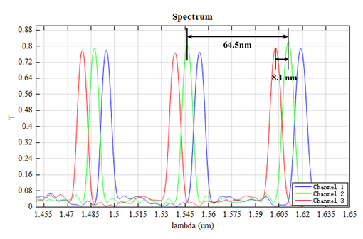
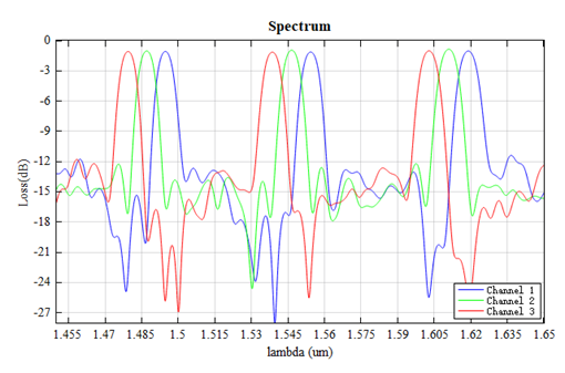
下图为三个输出波导中的FDFP监视器得到的透射率随波长的分布图,可以看到该器件的信道间隔为 ,自由频谱宽度为 ,与设计基本相符。
画出三个输出波导中得到的损耗随波长的分布如下图,可以看出,该器件的插入损耗为 ,串扰低于 。
参考文献
黄华茂. 基于硅纳米线的阵列波导光栅研究[D]. 华中科技大学, 2010. ↩︎