等离激元超材料红外吸收器
前言
“超材料(Metamaterial)”是一种特殊的人造材料,它们可以呈现出天然材料所不具备的超常物理性质,例如调控电磁波的频率、幅度、相位等。超材料的奇异特性使它具有广泛的应用前景,比如基于超材料设计的完美吸收器可以用作光电探测器,微辐射热计和热成像等。本案例根据 等人的工作[1],建模仿真了 Metal-Insulator-Metal(MIM)的等离激元超材料红外吸收器,研究其在可见光到近红外波段的反射透射吸收特性。
仿真设置
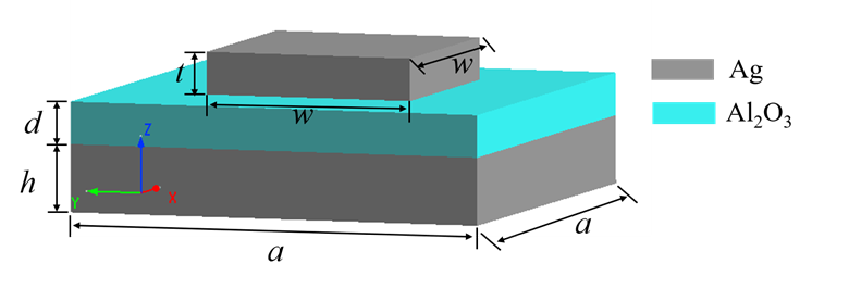
本案例中使用了一种由银-氧化铝-银组成的 MIM 结构。下层为银和氧化铝的无限大平板,上层是呈周期性排列的银立方体。其一个周期内的结构如下图所示,在光学仿真中我们只需要模拟其一个单元即可。由于结构和平面波光源的对称性,我们在 方向上使用Anti-Symmetric反对称边界条件;在 方向上使用Symmetric对称边界条件。使用对称和反对称边界条件可以缩小仿真空间从而减少仿真时间。
| 参数 | |||||
|---|---|---|---|---|---|
| 尺寸 |
材料设置
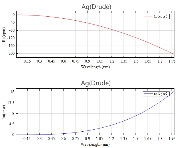
本案例中使用的金属为使用 Drude 模型建立的 Ag 材料,关于 Drude 模型的具体细节请参考Debye、Drude、Lorentz 材料:
其中, ,等离子频率 ,碰撞频率 。由 Drude 模型计算出的 Ag 的介电常数的实部和虚部如下图。
仿真结果
反射、透射和吸收率
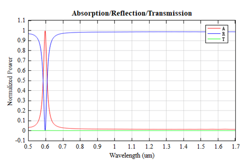
根据 MIM 红外吸收器顶部和底部的Frequency-Domain Field and Power(FDFP)频域场-功率监视器得到的 T 数据,绘制出吸收器的反射率(R)透射率(T)吸收率(A)的图像,结果如下图所示,波长在 左右,吸收器的吸收率达到峰值( 以上),其结果与参考文献中的Figure 2高度一致。
电场和电阻热分布
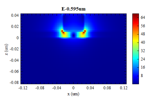
下图为 MIM 红外吸收器在波长为 时的电场分布。可以看出,在上层的银立方体与氧化铝的交界面处出现了电场增强效应。这是因为此处产生的表面等离子体激元共振将电场束缚在了此狭小区域。
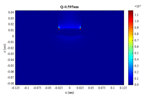
电阻热公式如下:
其中, 为光速, 为真空介电常数, 为介电常数的虚部,为电场强度。MIM 红外吸收器在波长 处的电阻热分布图如下。可以发现,电阻热 大部分局限在上层的 Ag 立方体和氧化铝交界面的棱角处,较高的吸收率使得此波长下大部分能量通过损耗转化成了热能。
参考文献
Hao J, Zhou L, Qiu M. Nearly total absorption of light and heat generation by plasmonic metamaterials[J]. Physical Review B Condensed Matter, 2011, 83(16):5919-5926. ↩︎
相关视频