利用线缺陷的光子晶体光学开关
前言
近年来,人们对光子晶体的异常色散的研究越来越感兴趣,通过适当地选择光子晶体的色散特性,可以实现例如超透镜、自准直、负折射等效应。其中自准直效应是指入射光沿晶体的某一特定方向传播时几乎没有衍射达到准直出射的效果。在二维光子晶体中,线缺陷会导致自准直光束的弯曲和分裂。在本案例中,我们通过改变光子晶体中的线缺陷(介质棒的半径)来实现“光学开关”的作用。
仿真设置
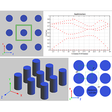
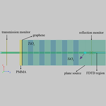
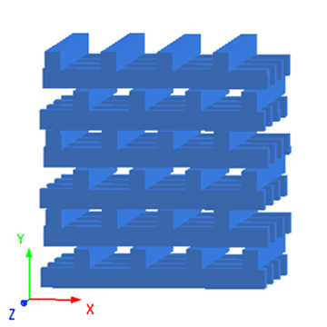
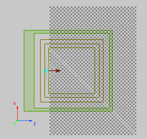
本案例中使用的二维光子晶体由半径 、介电常数为 12 的介质棒组成。其晶格常数 ,所有边界都使用完全匹配层(PML)吸收边界。通过控制仿真区域对角线上介质棒的半径,我们就可以为该晶体制造一个线型的缺陷。由参考文献 1 中得知,波长 的光沿着该晶体的晶格方向传播时会出现自准直效应,所以我们使用波长为 的高斯光束从晶体的左侧入射。
仿真结果
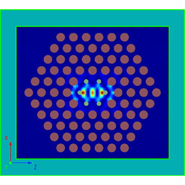
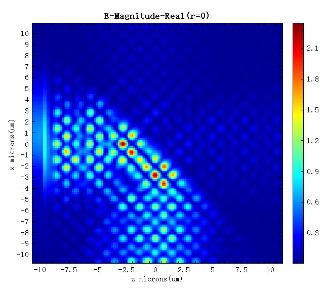
如下图所示,当对角线上介质棒的半径为 时,该光子晶体没有缺陷,光束在沿着其传播时几乎没有衍射现象,实现了自准直效应;当对角线上介质棒的半径为 0 时,光束在对角线(即线缺陷)处完全反射。该仿真现象与参考文献[1]中的图 2 一致。
参数分析
运行工程中的参数化扫描,对光子晶体的线缺陷(介质棒半径)进行扫描。扫描结束后,运行脚本,可以绘制出归一化后反射/透射功率随线缺陷(介质棒半径)变化的函数关系图:
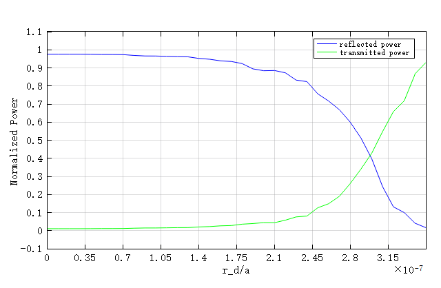
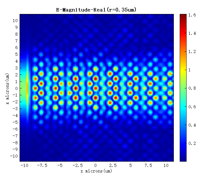
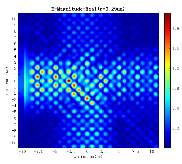
可以看出,线缺陷半径 时,光束经过结构后,在线缺陷处几乎全部反射;当线缺陷半径 时,光束经过结构后一半反射一半透射;随着线缺陷半径逐渐增大到 ,光子晶体变为完美周期性光子晶体时,光束经过结构可以全部透射。因此,通过调节线缺陷半径,我们能够操控光束的传播方向,实现“光开关”的功能。下图为线缺陷半径 时的电场分布,显示入射光半透半反,与上图中得到的结论一致。
参考文献
Lee et al., "Line-defect-induced bending and splitting of self-collimated beams in two-dimensional photonic crystals", App Phys Let 87, 181106 (2005) ↩︎
相关视频