负折射率传输线移相器
前言
在传统的传输线(TL)中,光信号的相速度小于群速度。随着光信号的传播,其相位会逐渐滞后。Antoniades等人提出了一种新型负折射率(NRI)的共面波导(CPW)传输线[1],它可以用在传统传输线后进行相位补偿,使得设计频率经过所有传输线传播后实现正、负或零相移。其负折射率超材料部分由集总元件电容器和电感器组成。与使用金属线带和开口谐振环实现负折射率相比,这种负折射率超材料的传播特性主要由集总元件决定。集总元件值的微小变化能在不改变总长度的情况下,改变传输线的相位特性。因此,与传统延迟线相比,其优点是体积小、结构简单、易于制作平面微波电路,在设计频率附近表现出线性相位响应。本案例参考了Antoniades等人的论文,建模仿真了工作频率 的零相移 NRI-TL。
仿真设置
结构设置
本案例使用的负折射率传输线的结构如下图所示,结构由放置在衬底上的一条中心导体带和两边的半无限大的导体平面组成。中心导体带作为信号传输线,两边的导体平面作为接地平面。中心导体带的宽度为 ,与两侧导体平面的间隙宽度为 。衬底的高度为 、相对介电常数为 。

在中心导体带上周期性的串并联了电容和电感元件如下图,其一个单元的长度为 ,串联一个 的电容,并联两个 的电感。电容器与信号线的宽度( )相同,长度为 。电感的长度与间隙( )相同,其宽度为 。

中心导体带与两边的导体平面的厚度相对于工作波长可以忽略不计,因此在仿真中可以使用 2D 矩形来模拟。根据Antoniades等人的论文[1:1],频率为 的光信号经过该结构后可以实现 0° 相位移动。
材料设置
NRI-TL 结构中,中心导体带和接地导体平面可以使用理想电导体(PEC)材料来模拟,电容和电感元件可以使用RLC材料。RLC材料用于指定具有给定电阻(R)、电感(L)、电容(C)的集总元件。当二维结构选择材料为 RLC 时,可以在该对象的材料选项卡中定义,如下图。RLC 材料不会出现在材料库中。须注意,电容器的电流方向为 轴方向,电感的电流方向为 方向。

监视器设置
下图展示了四个 CPW 单元级联时的仿真结构图,FDFP监视器 T1 位于 Port 光源与第一个 CPW 单元中间,用于测量光源注入的基模功率。FDFP监视器 T2 放置在第四个 CPW 单元后面,与 T1 监视器的距离为 。T2 监视器用于测量光信号穿过 CPW 结构后基模的功率。T1 和 T2 均需要打开模式扩展功能,模式扩展功能可以通过计算重叠积分来分析传输到非吸收波导的任意模式的功率比例,更多细节请参考模式扩展。

仿真结果
单级结构仿真
仿真结束后,附件中的NRI_TL_phase_shifter.msf脚本可以自动计算出光信号经过 NRI-TL 后的相移并与理论对比,如下图。理论计算时需要使用到传输线的 ,该值从FDFP监视器的解模得到的有效折射率计算得到:
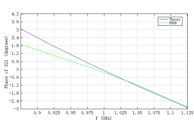
从图中可以看出,理论计算与仿真出的结果非常接近,理论计算出的零相移频率为 ,仿真得到的零相移频率为 ,与设计值 相差不到 2%。
多级结构仿真
附件中的NRI_TL_phase_shifter_sweep.msf脚本可以自动创建并运行三个工程文件,分别为单级 CPW 单元、2 级 CWP 单元串联和 4 级 CWP 单元串联的工程。仿真结束后,脚本还将自动计算出每个工程中得到的相移结果,并生成仿真结果与理论结果对比的曲线图如下。
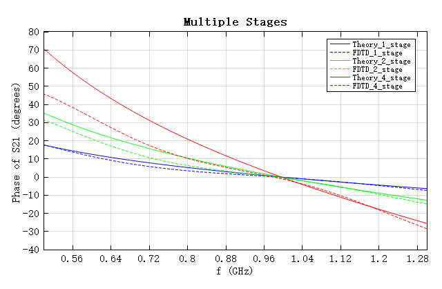
显然,随着 CPW 级数的增加,相位的斜率也会增加,可以实现更大的相移。仿真结果和理论计算出的零相移频率分别为 和 ,误差小于 2%,且与级数无关。这个现象完全符合论文[1:2]中的结论。