多模干涉耦合器
前言
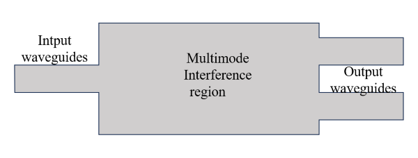
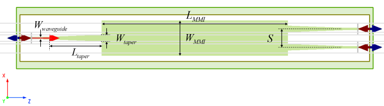
多模干涉(Multimode Interference,MMI)耦合器由输入波导、输出波导和多模干涉区三个部分构成。光场经由输入波导注入到多模干涉区后,多个模式间相长性干涉产生自镜像效应(self-imaging effect),沿导波的传播方向将周期性地产生输入场的一个或多个像。通过这个效应,该器件可以实现光的波分复用/解复用(Wavelength Division Multiplexing)、功率分配(Power Division)、偏振分束(Polarizing Splitter)等功能。
-
自镜像效应
自镜像效应是多模干涉器的理论基础。根据该理论,1 N 的对称型多模干涉耦合器的干涉区域长度一般就是首个 N 重像的位置,其计算公式如下:其中 ,其中 分别为基模和一阶本征模的传播常数, 是波导的折射率, 是 MMI 波导的宽度。具体细节请参考文献[1]。
在本案例当中,在输入/输出波导连接 MMI 区域的之间平滑地接入一段楔形波导(taper waveguide),可以大大减小纵向多模对成像均匀性的影响,同时降低在单模波导与 MMI 区域连接处产生反射而引起的附加损耗。此时,波导、楔形结构及 MMI 区的尺寸参数均影响着器件的性能,设计过程中往往不能确定每个结构的尺寸,并且很难保证每一部分的最佳尺寸在整合之后仍是最优解。本案例使用优化与扫描功能对模型参数进行扫描分析,从而进一步优化参数和模型。
仿真设置
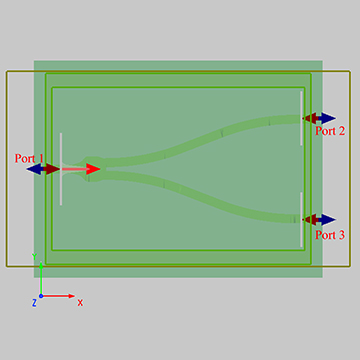
在本案例中,使用 3D FDTD 仿真,构建 1 2 端口的多模干涉耦合器。根据上述说明,器件的最短长度应当设置在首个二重像的位置。根据计算公式并参考文献[2],按照以下参数,如图所示构建器件。
| 参数名称 | 符号 | 尺寸 |
|---|---|---|
| 32 | ||
| 6 | ||
| 0.22 | ||
| 10 | ||
| 1.1 | ||
| 0.4 | ||
| 3.14 |
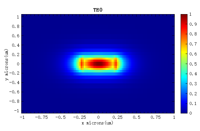
理论上,多模干涉耦合器对于 TE,TM 模式没有选择性,本案例当中,将使用 TE0 进行仿真。其模式场图如下所示
仿真结果
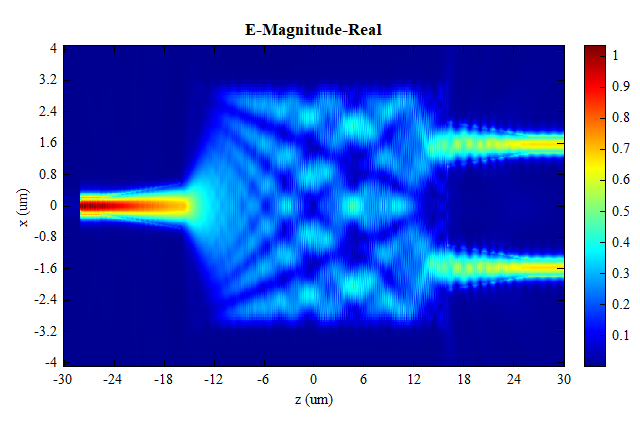
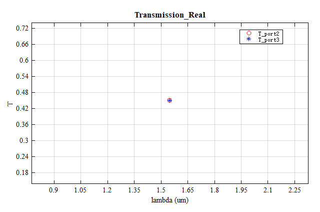
打开附件工程文件,直接运行,在Frequency-Domain Field and Power监视器的结果中,可以观察到入射光束在多模干涉区经过自镜像效应后,能量被均分到两个输出端口当中。此时两个输出端口中,透射率(port2 和 port3)完全相同。
参数分析
通常在单个工程仿真成功之后,可以新建参数扫描优化,得到某些参数对器件性能的影响,从而获取最优的器件设计。
多模干涉区的长度优化
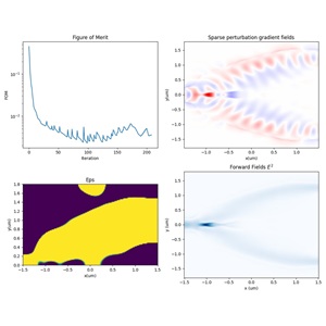
以理论公式计算得到的多模干涉区长度作为参考( ),本案例将会通过参数的优化与扫描功能来寻找最佳的多模干涉区长度。首先设置多模干涉区长度的扫描区间为 ,打开附件当中的工程,运行mmi_length的参数扫描,即可得到 port2 中的透射率随其变化的趋势,如下图所示,可以观察到最佳透射率应该在 到 之间。
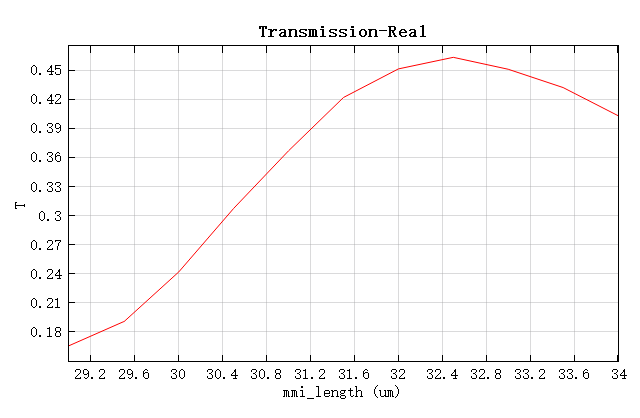
针对上述参数扫描结果,可以继续使用optimization对该参数进一步优化。优化所使用的默认算法为粒子群(Particle Swarm)算法 (见参考文献[3]) ,请注意选择进行目标函数的最大化还是最小化,即:Type 中选择Maximize还是Minimize,其它参数的意义具体参考Optimizations and Sweeps。
设置多模干涉区长度优化区间为 ,打开附件当中的工程,运行mmi_length_optimization优化,best fom表示优化得到的最大透射率,为 ,best parameters表示优化得到最佳多模干涉区长度,为 。其它参数意义具体参考Optimizations and Sweeps。
楔形结构的参数优化
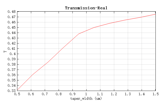
对于楔形结构的宽度,一方面增加其宽度,可以提高自成像的质量,从而降低器件损耗;另一方面,由于器件十分紧凑,两个输出波导之间间隔很小,为了防止输出波导之间的耦合串扰,楔形结构的宽度应该尽量小。本案例对其进行参数扫描,以便选择出最优解,扫描范围为 。打开附件工程,运行taper_width参数扫描,其结果如下图所示。在考虑两个输出波导之间的间距后,用户可以根据所需要的透射率要求,自行选择合适的楔形结构的宽度。
参考文献
Soldano L B , Pennings E C M, "Optical multi-mode interference devices based on self-imaging: principles and applications," Journal of Lightwave Technology. 13(4):615-627 (1995) ↩︎
D. J. Thomson, Y. Hu, G. T. Reed and J. -M. Fedeli, "Low Loss MMI Couplers for High Performance MZI Modulators," in IEEE Photonics Technology Letters, 22(20),pp.1485-1487 (2010). ↩︎
J. Robinson and Y. Rahmat-Samii, "Particle swarm optimization in Electromagnetics," IEEE Trans. Antennas and Propagat. 52, pp.397 - 407 (2004). ↩︎