使用交替相移掩模的光刻技术
前言
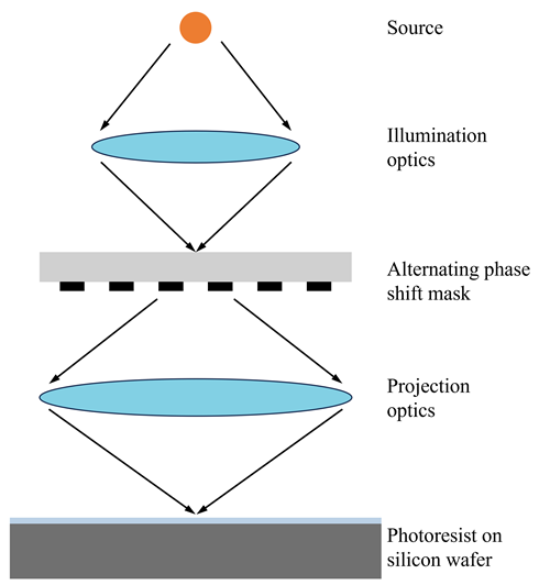
对更小、更快、更低功耗半导体器件的需求不断推动着光刻技术的进步。随着半导体器件尺寸的不断缩小,例如在 节点一些需要成像的特征小于所用的 光源的衍射极限,需要使用交替相移掩模(APSM)来提高分辨率。APSM对相位的调制,使得光线通过掩模后相互干涉,使掩模图案的边缘更为清晰锐利,从而提高图案的对比度。在亚波长尺度上产生的邻近效应需要通过光刻仿真来了解,以便在掩模设计中将其考虑在内,从而实现可预测的可靠的工艺。本案例展示了如何在FDTD中使用交替相移掩模(APSM)对亚波长特征进行成像。
仿真设置
模型简介
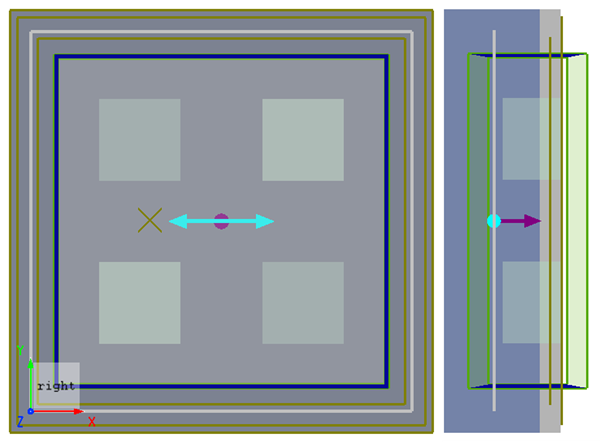
本案例使用的APSM的结构如下图,上层为带有棋盘式方格窗口的铬合金APSM,下层为玻璃基底。铬合金APSM上的每个方格窗口的边长为 ,在处于斜对角位置的窗口下方,玻璃基底被刻蚀出一定深度,使得通过交替刻蚀窗口传播的光波之间具有 的相位差。

FDTD求解器在 方向上使用Periodic周期性边界条件, 方向使用PML吸收边界。使用周期性边界可以只通过一个周期的仿真得到在该方向上无限周期的仿真结果。使用波长为 的平面波来模拟经过照明透镜后的ArF准分子激光,光源的偏振方向为 轴方向,如下图。
仿真结果
FDTD仿真使用时域有限差分算法严格求解透过掩模后的近场电磁场。所有折射、衍射、干涉、吸收和偏振效应都在掩模的近场中计算,而掩模的空间像则需要通过对FDTD仿真数据进行后处理得到。
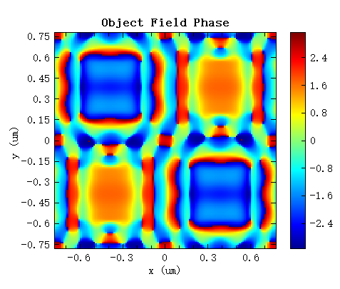
近场分布
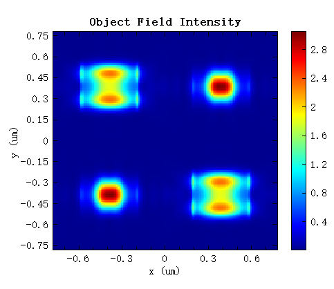
仿真结束后,运行分析组的分析脚本,绘制出铬合金APSM上表面处近场电场的场强和相位,如下图。可以看出每个窗口透射出的光强度变化明显,且相邻窗口之间具有 的相位差。
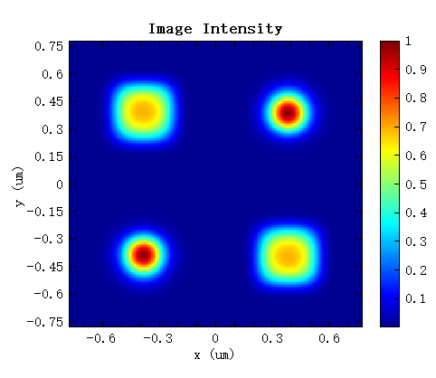
空间像
分析组的分析脚本还会自动对近场数据进行后处理,计算出在投影系统的数值孔径为 的时候,晶圆上形成的空间像,如下图:

为了使用FDTD严格计算在晶圆上的空间像,我们假设光源和照明光学采用科勒照明。使用科勒照明时,扩展光源上的点被假定为非相干辐射。光学系统的排列使得扩展光源上的任意点发出的光都以平面波的形式到达掩模,且每个点的入射角略有不同。因此对于圆形照明孔径,必须为每个正交偏振态执行一次仿真,并将结果按照强度相加。
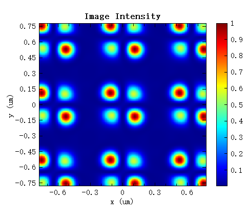
附件工程中包含了一个设置好的参数扫描,可以进行光源的偏振方向分别为 轴方向和 轴方向的两次仿真。运行参数扫描后,使用附件中的plot_incoherent.msf脚本可以绘制出叠加后的空间像,如下图:
接下来,将分析组中的缩小因子 设置为3后重新运行参数扫描和plot_incoherent.msf脚本。下图为绘制出的晶圆上的空间像。可以看到在缩小倍数 时,图像依然非常清晰,且背景干净。