聚焦光栅
前言
在许多数据通讯领域,高速光互连技术是进行大量数据交换的必要条件,因此光互连集成是近年来的热门研究课题。硅光集成技术以其优越的性能、低廉的成本以及易与其他光电元件单片集成等特点成为光互连集成最主要的候选技术。硅光集成的一个重要问题是集成波导器件与光纤或自由空间光学器件之间的接口问题,光栅耦合器凭借其易制作、灵活度高、对准容差大等优点,成为解决芯片与光纤之间耦合难题的最主要的解决方案。本案例根据 等人的工作[1],建模仿真了一个聚焦光栅,研究了该聚焦光栅的耦合损耗。
仿真设置
模型简介
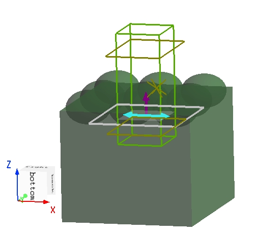
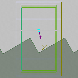
本案例中使用的聚焦光栅耦合器是基于浅刻蚀 技术,其波导层为 ,上下包层都为 ,衬底材料还是 ,如上图所示。 方向为光波导传输方向,光波导厚度方向为 方向。由于结构在 方向上对称,光源在 方向上反对称,因此我们在 方向上使用Anti-Symmetric反对称边界条件。
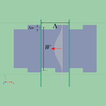
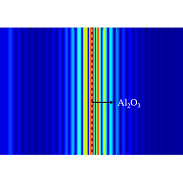
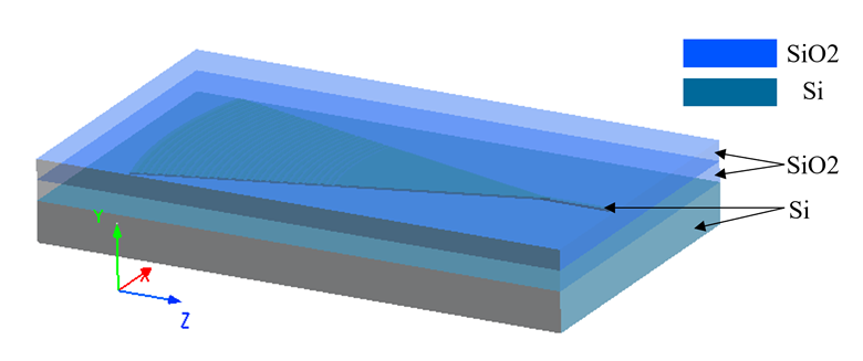
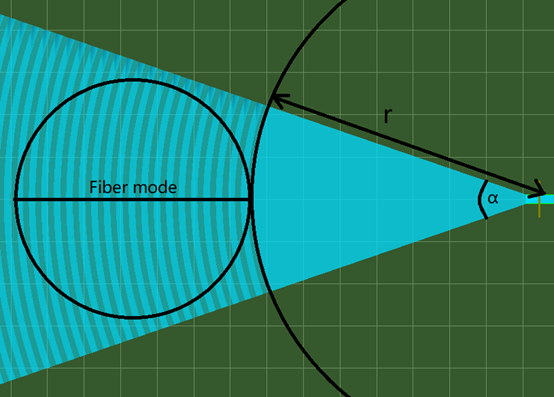
耦合光栅部分使用了共焦光栅,其工艺参数(波导厚度、埋氧层厚度、衬底厚度、包层厚度、浅蚀深度)使用 IME 规定的参数,光栅周期、占空比和 taper 的设计参考了文献[1:1]。如下图所示,光栅本身将光聚焦到宽度 的硅线波导中,其中 taper 的张角为 , 为 ,在设计中,光栅图案为同心圆线,圆心位于与波导相交的楔形物的顶点。
| Variables | Period/ | Duty |
|---|---|---|
| Value | 0.67 | 0.53 |
光源设置
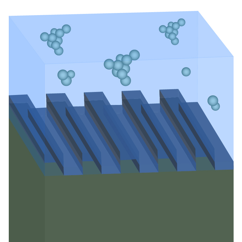
聚焦光栅接受到的入射光通常由阶跃型单模光纤传出,该入射光离开光纤后直接进入光栅结构顶部的玻璃包层。由于阶跃型单模光纤的出射光可以近似为高斯光源的场分布,所以在本案例的仿真工程中不对阶跃型单模光纤部分进行建模,仅将光纤的出射光用高斯光束代替。因此,在软件中设置高斯光源时,需要注意:
- 高斯光源的束腰尺寸与实际使用的光纤纤芯尺寸匹配;
- 高斯光源束腰面位置即代表光纤与光栅顶部包层的接触面位置,需要将光源所在的背景材料设置为Silica(玻璃)。
仿真结果
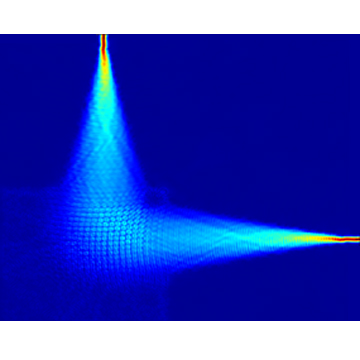
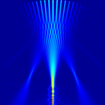
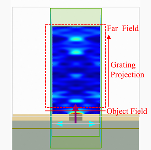
下图显示了放置在聚焦光栅耦合器中的FDFP监视器中得到的波长为 时的电场分布图,可以看到高斯光源的光入射到光栅区域后,被光栅耦合到右侧的硅线波导中。

下图为高斯光源距离硅线波导 处时,硅线波导中的FDFP监视器得到的透射率随波长的分布图,从图中可以看出,该聚焦光栅耦合器在波长为 处能够达到最大的透射率,为 。

参数分析
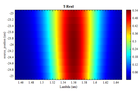
附件中的工程包含一个设置好的参数化扫描,可以对光源距离硅线波导从 到 之间的范围进行扫描。扫描结束后可以得到透射率 T 随光源位置变化的分布图,如下图。从图中可以看出,当光源距离硅线波导 时,该聚焦光栅耦合器可以在波长为 处达到最大的透射率,为 。