磁光波导的能带结构
前言
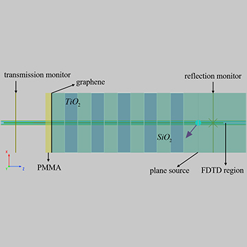
对于在传播方向上结构不变或者具有周期性的结构,我们可以使用 FDE 求解器解模。但是对于复杂材料组成的结构,如各向异性材料或非线性材料,我们使用 FDTD 求解器对其色散特性和能带结构进行求解。本案例构建了在传播轴向具有周期性结构的光波导模型,分别分析了由各向同性材料和对角各向异性材料组成的波导结构的能带。
仿真设置
模型简介
本案例使用 FDTD 求解器分析由各向同性和各向异性材料组成的光波导的能带结构。与各向同性材料不同的是,各向异性材料在各个方向上的介电常数不相等,这将会打破模式之间的简并性,计算得到的能带结构会发生明显变化。直波导在传播轴向上无限延伸,其结构可认为是周期性的,因此在 Z 方向上使用周期性边界条件。
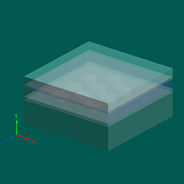
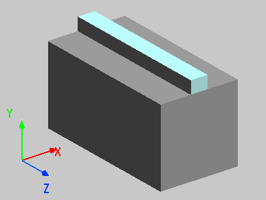
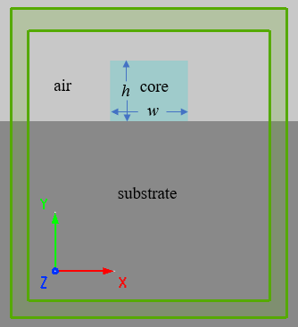
本模型中各向同性波导芯的折射率为 1.5。如图所示,直波导宽度 为 2.6 μm,高度 为 2 μm,沿 Z 轴向无限延伸。波导基底选择折射率为 1.4 的介质材料。
模型构建
仿真模型的组件等详细信息见附件工程文件 nr_waveguide3d.mpps。一般地,为了计算目标结构完整的能带结构,必须使用偶极子源阵列作为输入源,并设置目标频段,这些设置已经在能带结构相关案例中进行了详细介绍。(相关的能带结构仿真案例详细介绍见2D 正方晶格能带结构。)但是对于本案例,我们目标是寻找波导材料对模式的影响,仅需要观测到由波导系统变化对能带结构的影响,所以我们在这里使用模式源来代替偶极子源阵列。模式源可以求解入射模式,这将更快速地获得最终结果。求解模式可以发现本案例中的波导支持 TM 和 TE 两种模式,由于这两种模式是正交的,所以我们构建两个模式源分别注入 TE 和 TM 两种模式,并在 1.5 μm 到 1.6 μm 的波长范围内求解并观测这两种模式。
仿真结果
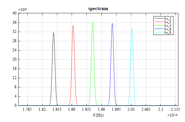
附件 nr_waveguide3d.mpps 为本案例的展示文件,下载后并点击运行,可以得到特定波矢下的共振频谱。运行参数扫描,得到不同波矢 下的共振频谱。为了加快运算速度并得到结果,仅从 范围内选择 5 个点。运行参数扫描可以计算得到 5 个不同波矢下的共振频谱图。运行完成之后,加载并运行 nr_waveguide3d.msf 文件,可以计算出有效折射率和传播常数。
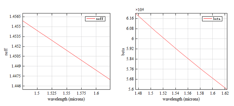
首先,我们仿真各向同性材料组成的规则波导,波导芯的材料设置为折射率为 1.5 的介质材料。运行参数扫描后,打开 nr_waveguide3d.msf 文件并运行。有效折射率可计算为 ,其中 为真空中的波数。最终计算得到的有效折射率、传播常数与波长的关系如图所示。
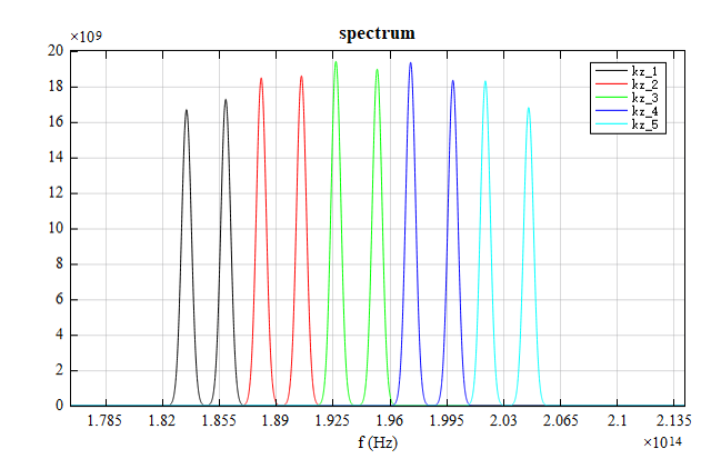
不同波矢下的共振频谱如下图所示。由频谱可知,在各向同性的波导下,模式简并导致每个波矢 下只有一个共振峰。
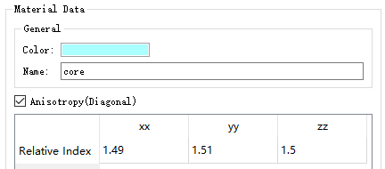
接下来,进行各向异性材料波导的计算。在软件主界面中点击Materials进入Material Library界面,在 Material List 中点击“Go to Project Material Library”进入工程材料库页面,左键双击材料“core”进入材料的编辑界面,在这里选择勾选框 Anisotropy(Diagonal),使用对角各向异性材料。在对应的输入框中输入对角各向异性材料的折射率 、 、 分别为 1.49、1.51、1.50,设置完成后点击保存,如图所示。
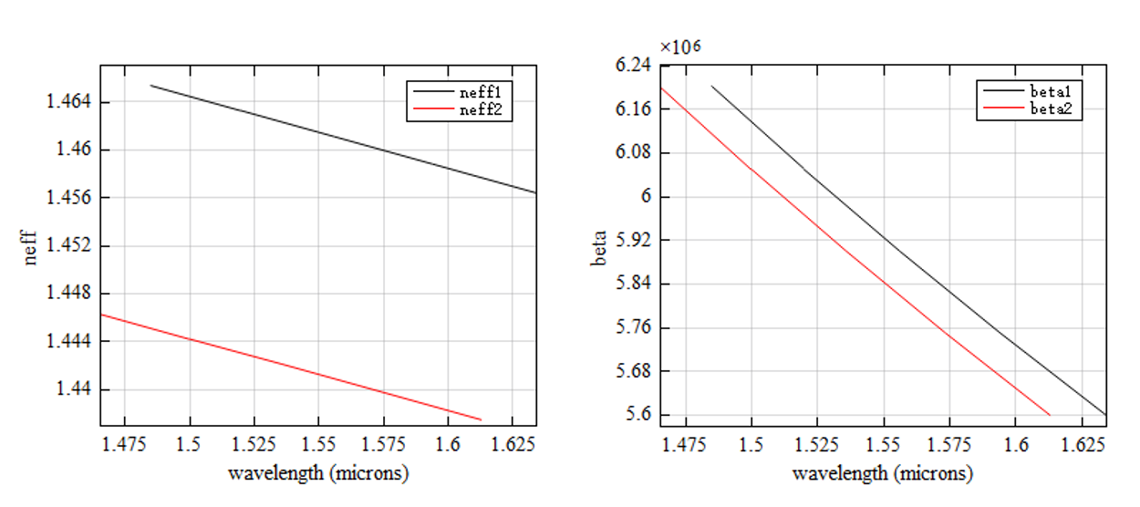
重新运行仿真,即可得到各向异性波导在特定波矢下的频谱。再次运行参数扫描后,运行附件脚本查看各向异性波导模型的计算结果。如下图所示,对应两个不同模式的有效折射率和传播常数均存在明显差值。
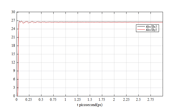
波导中心的 time monitor 记录了波导中的电场信号随时间变化情况。其中 、 的振幅如下图所示,可以看出两个模式之间并没有发生耦合,这是因为这两个模式之间是正交的。
如下图所示,原本频谱中仅有单个共振峰,现在变成了两个。说明有两个共振频率分别对应于两个模式。这是由于各向同性模型中 TM 和 TE 模式的简并性被打破。