3D立方晶格能带结构
前言
3D 立方晶格(3D Cubic Lattice)是 3D Rectangular Lattice 中的一种特例,此类型光子晶体的晶格间距在空间内三个轴向均相等。本案例构建了 3D 立方晶格光子晶体几何模型,使用 FDTD 求解器进行仿真计算,分析介质球 3D 立方晶格光子晶体的能带结构。
仿真设置
模型简介
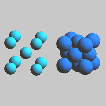
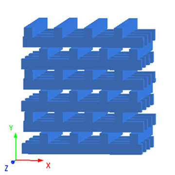
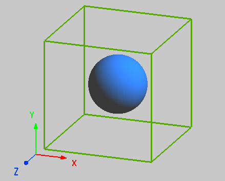
本案例使用 FDTD 分析由均匀介质球周期排列组成的立方晶格光子晶体的能带结构。与 2D 正方晶格光子晶体类似,介质球在空气中周期排列实现了空间中周期性变化的折射率分布,形成了光子带隙。对于本模型,周期性排布的介质球体的半径 为 0.13 μm,介质材料的折射率为 3.00,背景为空气,立方晶格的晶格间距 为 0.5 μm。
模型构建
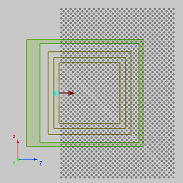
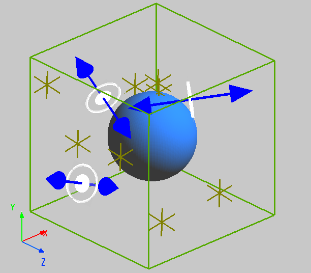
本案例的仿真设置与2D 正方晶格能带结构案例相似,附件 3D_cubic.mpps 为本案例的展示文件,打开文件后可以看到详细的模型参数及设置。3D 立方晶格结构在空间中三个轴向均呈周期性变化,需要使用 3D FDTD 仿真。通过调节 FDTD 的几何中心坐标及轴向范围将仿真区域设置为与 3D 立方晶格的周期单元区域相同,此时结构单元位于仿真区域中心,如下图所示。为了使结构单元模型体现出周期性分布,在 z、x 和 y 轴向的边界均使用 Bloch 周期性边界条件。使用分析组 Dipole Clouds 和 bandstructure 构建 3D FDTD 仿真区域中位置随机的多个偶极子源及 time monitor,注意在分析组 Dipole Clouds 中将晶格类型变量更改为 3(3D rectangular lattice)。
仿真结果
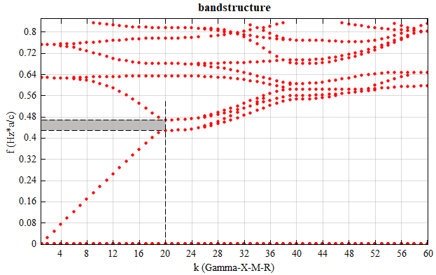
下载并打开附件 3D_cubic.mpps,手动运行所有的参数扫描。完成对波矢的参数扫描后,下载本光子晶体案例对应的能带结构计算脚本文件 3D_cubic.msf 并运行,即可得到能带结构图,如下图所示,此光子晶体的禁带范围为图中阴影区域。